As a Wafer Fab Specialist, the individual is responsible for performing fabrication or electrical wafer test operations. The job description entails setting up, operating, loading, and monitoring a machine and equipment to inspect and verify the quality of the product that is being produced. Other related work activities are listed on the Wafer Fab Specialist Resume as – recording and analyzing data, cutting wafers into individual pieces which hold multiple chips, loading the wafer equipment, ordering supplies, and performing quality control testing.
To ensure success the following job assets will prove to be useful – physical fitness, attention to details, attention to safety, stamina, time management, and manual dexterity. Some employers necessitate an associate’s degree for this position, while it is not mandatory. Work experience may prove to be useful while compared to formal education.
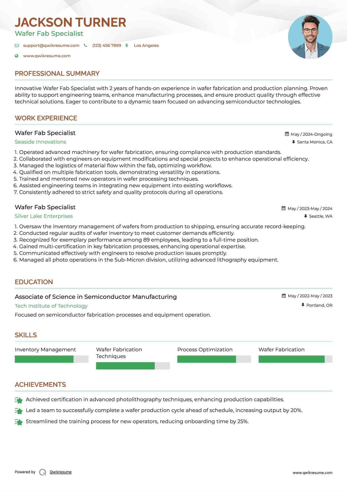
Objective : Innovative Wafer Fab Specialist with 2 years of hands-on experience in wafer fabrication and production planning. Proven ability to support engineering teams, enhance manufacturing processes, and ensure product quality through effective technical solutions. Eager to contribute to a dynamic team focused on advancing semiconductor technologies.
Operated advanced machinery for wafer fabrication, ensuring compliance with production standards.
Collaborated with engineers on equipment modifications and special projects to enhance operational efficiency.
Managed the logistics of material flow within the fab, optimizing workflow.
Qualified on multiple fabrication tools, demonstrating versatility in operations.
Trained and mentored new operators in wafer processing techniques.
Assisted engineering teams in integrating new equipment into existing workflows.
Consistently adhered to strict safety and quality protocols during all operations.
Experience
0-2 Years
Level
Entry Level
Education
A.S. in S.M.
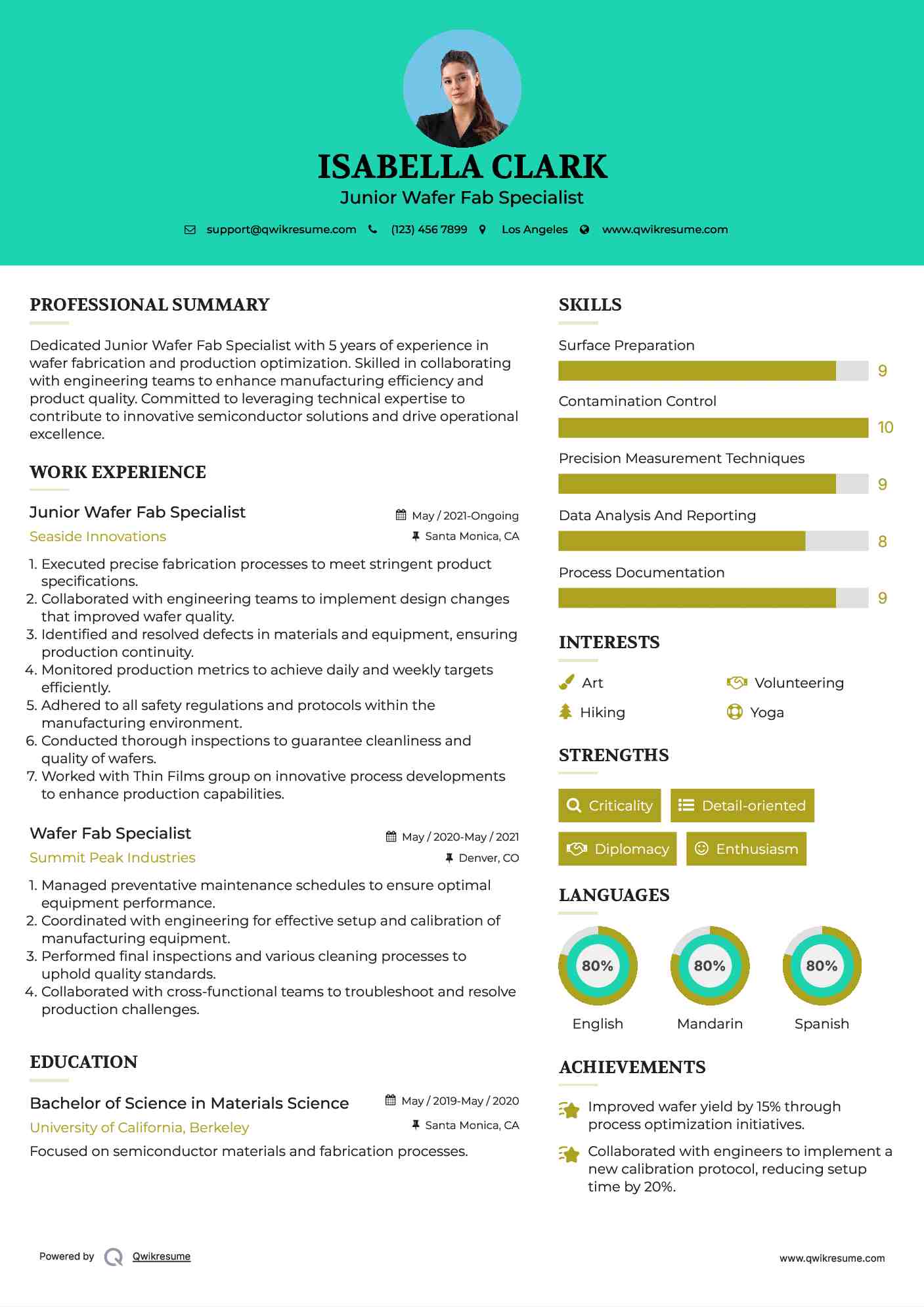
Junior Wafer Fab Specialist Resume
Objective : Dedicated Junior Wafer Fab Specialist with 5 years of experience in wafer fabrication and production optimization. Skilled in collaborating with engineering teams to enhance manufacturing efficiency and product quality. Committed to leveraging technical expertise to contribute to innovative semiconductor solutions and drive operational excellence.
Skills : Surface Preparation, Contamination Control, Precision Measurement Techniques, Data Analysis And Reporting, Process Documentation
Description :
Executed precise fabrication processes to meet stringent product specifications.
Collaborated with engineering teams to implement design changes that improved wafer quality.
Identified and resolved defects in materials and equipment, ensuring production continuity.
Monitored production metrics to achieve daily and weekly targets efficiently.
Adhered to all safety regulations and protocols within the manufacturing environment.
Conducted thorough inspections to guarantee cleanliness and quality of wafers.
Worked with Thin Films group on innovative process developments to enhance production capabilities.
Experience
2-5 Years
Level
Junior
Education
B.S. in Materials Science
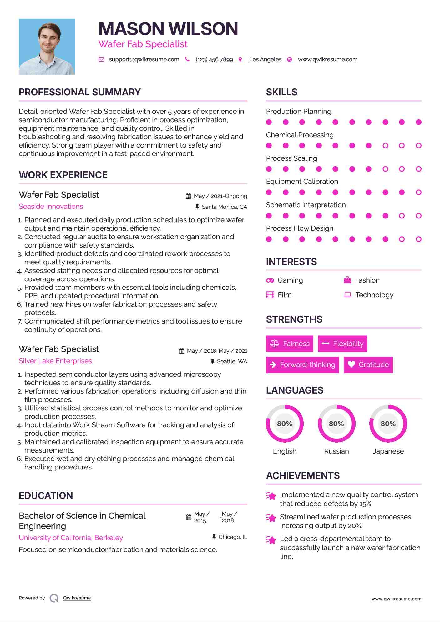
Wafer Fab Specialist Resume
Headline : Detail-oriented Wafer Fab Specialist with over 5 years of experience in semiconductor manufacturing. Proficient in process optimization, equipment maintenance, and quality control. Skilled in troubleshooting and resolving fabrication issues to enhance yield and efficiency. Strong team player with a commitment to safety and continuous improvement in a fast-paced environment.
Skills : Production Planning, Chemical Processing, Process Scaling, Equipment Calibration, Schematic Interpretation, Process Flow Design
Description :
Planned and executed daily production schedules to optimize wafer output and maintain operational efficiency.
Conducted regular audits to ensure workstation organization and compliance with safety standards.
Identified product defects and coordinated rework processes to meet quality requirements.
Assessed staffing needs and allocated resources for optimal coverage across operations.
Provided team members with essential tools including chemicals, PPE, and updated procedural information.
Trained new hires on wafer fabrication processes and safety protocols.
Communicated shift performance metrics and tool issues to ensure continuity of operations.
Experience
5-7 Years
Level
Senior
Education
B.S. Ch.E.
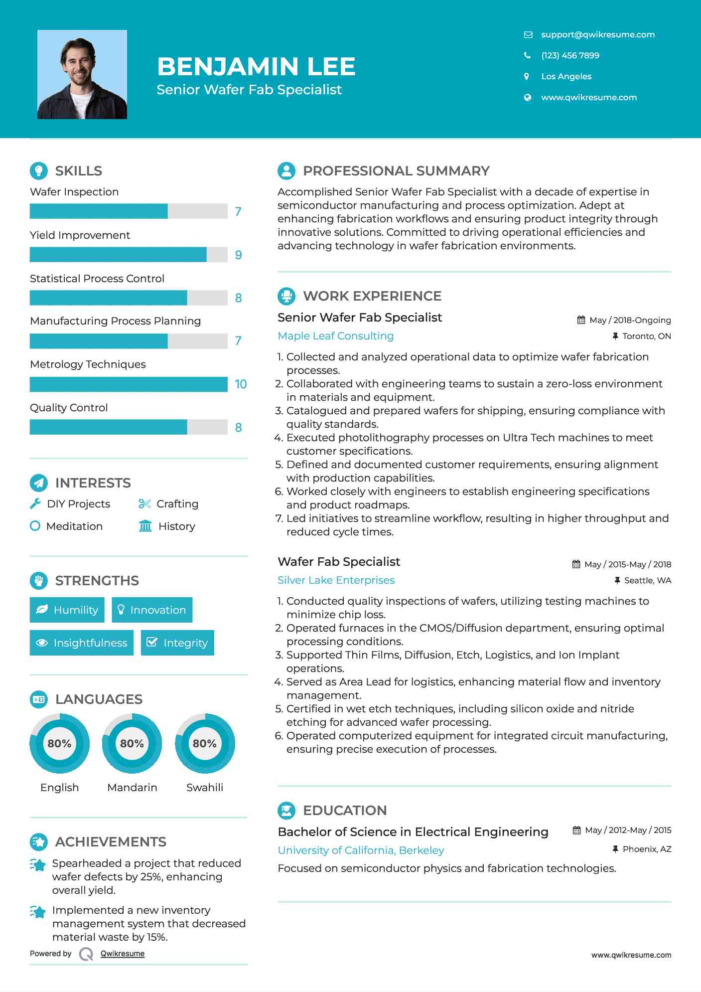
Senior Wafer Fab Specialist Resume
Summary : Accomplished Senior Wafer Fab Specialist with a decade of expertise in semiconductor manufacturing and process optimization. Adept at enhancing fabrication workflows and ensuring product integrity through innovative solutions. Committed to driving operational efficiencies and advancing technology in wafer fabrication environments.
Skills : Wafer Inspection, Yield Improvement, Statistical Process Control, Manufacturing Process Planning, Metrology Techniques, Quality Control
Description :
Collected and analyzed operational data to optimize wafer fabrication processes.
Collaborated with engineering teams to sustain a zero-loss environment in materials and equipment.
Catalogued and prepared wafers for shipping, ensuring compliance with quality standards.
Executed photolithography processes on Ultra Tech machines to meet customer specifications.
Defined and documented customer requirements, ensuring alignment with production capabilities.
Worked closely with engineers to establish engineering specifications and product roadmaps.
Led initiatives to streamline workflow, resulting in higher throughput and reduced cycle times.
Experience
7-10 Years
Level
Management
Education
BSEE
Wafer Fab Specialist Resume
Summary : Seasoned Wafer Fab Specialist with 10 years of extensive experience in semiconductor fabrication and process optimization. Expertise in enhancing production workflows, ensuring quality control, and implementing innovative solutions to drive efficiency. Passionate about contributing to cutting-edge semiconductor technology in a collaborative team environment.
Skills : Training And Mentoring, Process Simulation Software, Database Management For Manufacturing, Manufacturing Execution Systems (mes), Cleanroom Safety, Chemical Etching
Description :
Processed wafers for semiconductor production, ensuring adherence to strict quality standards.
Utilized troubleshooting skills to enhance fab performance and resolve process-related issues.
Obtained certifications in advanced fabrication techniques, including backside processes.
Executed preventative maintenance and upgrades on critical production equipment.
Optimized tool performance, addressing process requirements and minimizing equipment downtime.
Collaborated with engineering teams to enhance manufacturing processes and product quality.
Trained new personnel on fabrication techniques and safety protocols.
Experience
10+ Years
Level
Executive
Education
BSEE
Lead Wafer Fab Specialist Resume
Headline : Dynamic Lead Wafer Fab Specialist with 7 years of extensive experience in semiconductor fabrication and process optimization. Proven expertise in enhancing yield, managing complex workflows, and ensuring product quality through innovative solutions. Committed to driving operational excellence and advancing semiconductor manufacturing technologies in a collaborative environment.
Skills : Data Analysis, Cleanroom Protocols, Troubleshooting Skills, Chemical Handling
Description :
Supervised tool utilization and post-maintenance to ensure optimal performance metrics were achieved.
Utilized Section Manager Software (SMS) for effective tracking of production metrics and tool management.
Managed cycle times and prioritized materials through internal software, ensuring timely fulfillment of customer demands.
Generated detailed progress reports and maintained databases to document equipment and material issues.
Participated in Rapid Improvement Events (RIE) to enhance maintenance material efficiency, minimizing idle time.
Worked in cleanroom environments across multiple facilities, ensuring high standards of cleanliness and safety.
Executed tests on various machines during final phases of silicon wafer production, demonstrating strong troubleshooting skills.
Experience
5-7 Years
Level
Consultant
Education
BSEE
Wafer Fab Specialist Resume
Objective : Experienced Wafer Fab Specialist with a solid background in semiconductor processes and cleanroom protocols. Expertise in photolithography, etching, and deposition techniques. Proven track record of improving production efficiency and reducing defects. Excellent analytical skills and a strong focus on quality assurance, ensuring compliance with industry standards.
Collaborated with engineering teams to improve wafer production processes and ensure adherence to quality standards.
Executed production plans for semiconductor wafers, optimizing workflow and resource allocation.
Maintained and calibrated wafer fabrication equipment to ensure optimal performance.
Conducted regular quality checks to verify compliance with industry standards.
Operated and maintained semiconductor fabrication equipment for optimal performance.
Analyzed production data to identify areas for efficiency improvements.
Supported the implementation of process improvements that enhanced overall productivity.
Experience
0-2 Years
Level
Fresher
Education
BSEE
Junior Wafer Fab Specialist Resume
Objective : With 5 years of experience in wafer fabrication, I excel in optimizing production processes and maintaining high-quality standards. My expertise includes collaborating with engineering teams to troubleshoot and enhance manufacturing efficiency. I am driven to support innovative semiconductor solutions and contribute to the advancement of cutting-edge technologies.
Skills : Process Management, Team Collaboration, Production Scheduling, Technical Support, Technical Reporting, Data Analysis Tools
Description :
Managed production scheduling, ensuring timely delivery of wafers while adhering to quality standards.
Optimized inventory management systems, improving material availability and reducing waste.
Collaborated with cross-functional teams to align production goals with customer specifications.
Conducted thorough quality assurance checks to address and resolve any issues.
Ensured compliance with industry regulations and safety protocols, including FCC and TSMC standards.
Maintained strong communication with design teams to meet fabrication requirements effectively.
Trained new staff on fabrication processes and safety practices to ensure operational excellence.
Experience
2-5 Years
Level
Junior
Education
BSEE
Wafer Fab Specialist Resume
Summary : Seasoned Wafer Fab Specialist with over 10 years of experience in semiconductor manufacturing. Expert in process validation, quality assurance, and equipment optimization. Proven success in enhancing production efficiency and ensuring compliance with industry standards. Passionate about driving innovation in wafer fabrication and contributing to high-quality semiconductor solutions.
Skills : Process Monitoring, Thin Film Deposition, Etching Processes, Ion Implantation, Diffusion Processes, Photolithography
Description :
Collaborated with the WFA team to align manufacturing processes with customer specifications.
Provided comprehensive technical support for wafer fabrication, testing, and chip design.
Facilitated communication between design and fabrication teams to streamline product development.
Managed technical support functions for the Wafer Fab Team, driving process improvements.
Offered ongoing assistance for new product developments, ensuring alignment with quality standards.
Supported advancements in wafer technology, leading to enhanced process efficiencies.
Delivered customer service training focused on wafer technology applications and engineering design.
Experience
7-10 Years
Level
Freelancer
Education
BSEE
Wafer Fab Specialist Resume
Summary : Accomplished Wafer Fab Specialist with a decade of extensive experience in semiconductor fabrication and process enhancement. Demonstrated expertise in optimizing workflows, conducting quality assurance, and implementing innovative solutions to elevate production efficiency. Driven to contribute to groundbreaking semiconductor technologies in a collaborative and dynamic environment.
Skills : Process Flow Management, Time Management, Project Management, Root Cause Analysis, Tool Calibration
Description :
Collaborated with engineering teams to enhance wafer fabrication processes and ensure product specifications are met.
Conducted thorough inspections and testing of wafers before shipment, ensuring compliance with quality standards.
Implemented process improvements that increased efficiency and reduced waste in the production line.
Supported product development efforts by providing technical expertise and troubleshooting solutions.
Maintained proper storage and handling of materials for production processes.
Actively participated in cross-functional teams to drive continuous improvement initiatives.
Monitored inventory levels and analyzed data to optimize resource allocation.
Creating an account is free and takes five seconds.
You'll get access to the PDF version of this resume template.
Choose an option.
Sign up with Google
Sign up with Facebook
Sign up with Linkedin
This helps us make sure you're human and prevents spammers from abusing our services.
By continuing, you agree to our Privacy Policy and Terms.
Unlock the Power of Over 10,000 Resume Samples.
Take your job search to the next level with our extensive collection of 10,000+ resume samples. Find inspiration for your own resume and gain a competitive edge in your job search.
Get Hired Faster with Resume Assistant.
Make your resume shine with our Resume Assistant. You'll receive a real-time score as you edit, helping you to optimize your skills, experience, and achievements for the role you want.
Get Noticed with Resume Templates that Beat the ATS.
Get past the resume screeners with ease using our optimized templates. Our professional designs are tailored to beat the ATS and help you land your dream job.