The role of a PCB Designer is to design the circuit boards that are used mainly in technology-based products or devices. Typical work activities seen on the PCB Designer Resume include the following – develop and test PCB’s; using computer-aided design ( CAD tools) to build circuitry, developing both digital and analog designs, implementing design processes, placing components and conductors; testing designs, developing the layout of printed Circuit board test hardware; managing schematic capture and editing a variety of designs; and administering component generation and maintenance of component libraries.
The ideal candidate should demonstrate on the resume the following skills and abilities – experience in layout and assembling; sound knowledge of PADS Power PCB and Orcad Schematic Capture; in-depth knowledge of modern PCB manufacture and assembly techniques; and the ability to present all technical information in a clear and format. Employers pick resumes that denote an associate’s degree in the field of electronics engineering.
Objective : Innovative PCB Designer with 2 years of experience in designing high-performance circuit boards for diverse applications. Proficient in utilizing industry-standard tools to create efficient layouts and schematics while adhering to strict IPC standards. Eager to leverage technical expertise and creative problem-solving skills to advance product development and contribute to team success.
Executed PCB design for Analog, Digital, RF, and Power Supply boards, ensuring compliance with IPC standards.
Developed a 4-layer PCB layout for FPGA applications, optimizing signal integrity.
Collaborated closely with production teams to finalize PCB designs for clients such as GE Lighting and Samsung.
Designed and implemented LED driver circuits, meeting rigorous performance specifications.
Conducted design reviews and revisions based on feedback to enhance product reliability.
Utilized Altera FPGA technology to innovate circuit designs for improved functionality.
Maintained documentation of design processes for future reference and compliance audits.
Experience
0-2 Years
Level
Entry Level
Education
BSEE
Senior PCB Designer Resume
Headline : Accomplished Senior PCB Designer with over 7 years of experience in developing advanced circuit board solutions across various industries. Expertise in leveraging cutting-edge design software and IPC standards to optimize performance and reliability. Committed to enhancing product innovation through meticulous layout design and collaborative engineering efforts.
Designed and optimized multi-layer PCBs using advanced tools such as DxDesigner and PADS, ensuring compliance with IPC standards.
Collaborated with electrical engineers to develop schematics and layouts for complex electronic systems.
Conducted thorough design reviews and implemented engineering change orders (ECOs) to maintain project timelines.
Utilized simulation tools for signal integrity and thermal analysis, enhancing product reliability.
Managed component library and created custom footprints for unique parts to streamline the design process.
Coordinated with manufacturers to provide fabrication and assembly documentation, ensuring high-quality production.
Participated in R&D initiatives to innovate PCB designs that meet specific client requirements.
Experience
5-7 Years
Level
Senior
Education
BSEE
PCB Designer Resume
Objective : Dedicated PCB Designer with 2 years of hands-on experience in crafting reliable circuit boards for various applications. Skilled in utilizing advanced design software to optimize layouts and ensure compliance with IPC standards. Passionate about contributing innovative solutions and collaborating with cross-functional teams to elevate product development.
Conducted material selection and stackup design for effective PCB fabrication.
Performed design reviews addressing electrical, thermal, and mechanical constraints.
Collaborated with engineers to resolve manufacturing and packaging conflicts.
Utilized Altium Designer for schematic capture and PCB layout.
Engaged in multi-layer PCB design, ensuring adherence to IPC standards.
Executed power distribution network (PDN) design and routing.
Supported cross-functional teams in product development initiatives.
Experience
0-2 Years
Level
Junior
Education
BSEE
Assistant PCB Designer Resume
Objective : Technical PCB Designer with 2 years of experience specializing in high-quality circuit board layouts and schematics. Proficient in using industry-standard tools to address design challenges and enhance product performance. Committed to collaborating effectively with engineering teams to deliver innovative solutions that meet project specifications and timelines.
Resolved power distribution network (PDN) challenges, including plane bounce and EMI issues.
Implemented Engineering Change Notices (ECNs), developed symbols and footprints, and maintained libraries.
Assisted in schematic capture and PCB design under the guidance of a Senior Engineer.
Conducted quality testing for various sensor applications, ensuring compliance with specifications.
Collaborated with cross-functional teams to enhance design outcomes.
Utilized industry-standard software tools for efficient PCB design processes.
Supported prototype testing and validation to ensure design functionality.
Experience
0-2 Years
Level
Entry Level
Education
AAS Electronics
PCB Designer Resume
Objective : Driven PCB Designer with 2 years of experience in creating reliable circuit board designs for various applications. Adept at utilizing industry-standard design tools to develop precise layouts and schematics while ensuring compliance with IPC standards. Passionate about leveraging technical skills to enhance product functionality and contribute to innovative engineering solutions.
Skills : Autocad, Gerber File Generation, Bill Of Materials (bom), Documentation Skills, Technical Writing, Collaboration Skills
Description :
Utilized OrCAD for schematic capture and layout design, delivering high-quality PCB solutions.
Conducted routing, length matching, and generated Gerber files for manufacturing processes.
Verified electrical schematics against customer specifications, overseeing BOM creation and component procurement.
Designed 10-layer, double-sided high-density SMT PCBs with integrated RF, GPS, and Bluetooth controllers.
Executed pre and post-assembly board validation and debugging to ensure product integrity.
Collaborated with engineering teams to address design challenges and optimize PCB performance.
Experience
0-2 Years
Level
Fresher
Education
BSEE
PCB Layout Designer
Resume
Summary : Seasoned PCB Layout Designer with a decade of experience in crafting high-quality circuit boards across various industries. Expert in utilizing advanced CAD tools and adhering to IPC standards to deliver precise layouts and innovative designs. Proven ability to collaborate with cross-functional teams to enhance product performance and drive engineering excellence.
Skills : Pcb Fabrication And Assembly, Design For Manufacturability, Schematic Capture, Orcad Pcb Designer
Description :
Collaborated with mechanical engineers to address packaging challenges, ensuring optimal board form factors.
Processed Gerber files and provided design and manufacturing support to engineering teams.
Conducted pre- and post-design reviews to enhance design quality and functionality.
Introduced innovative design concepts while addressing electrical, thermal, mechanical, and manufacturing constraints.
Managed the routing of single-ended, 50-ohm RF and 100-ohm differential signals.
Executed design rule checks to ensure compliance with industry standards.
Provided training to junior designers on PCB layout best practices and tools.
Experience
7-10 Years
Level
Management
Education
BSEE
PCB Designer Resume
Objective : Accomplished PCB Designer with 5 years of hands-on experience in developing high-performance circuit boards tailored for advanced applications. Proficient in leveraging industry-standard design software and IPC standards to deliver accurate layouts and documentation. Committed to driving innovation and efficiency in product development through collaboration and technical expertise.
Skills : Collaboration Tools, High-speed Design, Multilayer Pcb Design, Analog Circuit Design, Digital Circuit Design, Power Distribution Networks
Description :
Managed all aspects of PCB design, including schematics, BOM, and prototype development, ensuring stringent documentation control.
Designed controlled impedance, multi-layer, and high-density PCBs tailored for specific application requirements.
Collaborated with external vendors and internal teams to streamline production and assembly processes.
Utilized Mentor Graphics Pads Layout software for precise PCB layout and design.
Compiled and maintained comprehensive project documentation for all PCB designs.
Designed with Capture 2007.9.2EE and Windchill TRC Technology Research Corp., enhancing design accuracy.
Demonstrated proficiency in PCB design and layout, achieving high-quality results consistently.
Experience
2-5 Years
Level
Consultant
Education
BSEE
PCB Design Engineer Resume
Headline : Results-oriented PCB Design Engineer with 7 years of experience in creating high-performance circuit boards across multiple industries. Skilled in utilizing advanced design software and adhering to IPC standards to ensure optimal functionality and reliability. Adept at collaborating with cross-functional teams to drive innovation and enhance product development.
Designed and optimized multi-layer PCBs for various applications, ensuring adherence to IPC standards.
Designed and developed PCB layouts for various electronic devices using industry-standard software.
Developed comprehensive documentation for PCB layouts and manufacturing processes.
Conducted design reviews to ensure compliance with industry standards and specifications.
Managed engineering changes efficiently, streamlining the design process.
Utilized simulation tools to validate PCB designs and improve reliability.
Mentored junior engineers in PCB design best practices and software usage.
Experience
5-7 Years
Level
Senior
Education
BSEE
PCB Designer Resume
Headline : Accomplished PCB Designer with 7 years of experience in developing innovative circuit board solutions for a variety of applications. Expertise in advanced design software and IPC standards, ensuring high-quality layouts and compliance. Passionate about driving product enhancements through collaborative engineering and technical excellence.
Collaborated with engineering teams to design high-performance circuit boards, ensuring compliance with specifications and industry standards.
Utilized Cadence Allegro for complex board layouts, ensuring optimal performance and manufacturability.
Executed PCB layout designs using FR-4 material, accommodating up to 10 layers and various copper thicknesses.
Developed and maintained documentation for design specifications, including Gerber and DXF files for fabrication.
Conducted design reviews and provided technical support throughout the lifecycle of PCB projects.
Implemented effective communication strategies with mechanical engineers to define board outlines accurately.
Managed project timelines and deliverables, ensuring quality and adherence to IPC standards.
Experience
5-7 Years
Level
Senior
Education
BSEE
PCB Designer Resume
Objective : Skilled PCB Designer with 5 years of experience in developing efficient and reliable circuit board designs for cutting-edge technologies. Adept in utilizing advanced design tools and adhering to IPC standards to produce high-quality layouts and documentation. Passionate about leveraging technical expertise to drive innovative solutions and collaborate effectively within engineering teams.
Skills : Manufacturing Processes, Pcb Assembly Processes, Soldering Techniques, Testing And Validation, Communication Skills
Description :
Designed and developed circuit boards from specifications, ensuring adherence to IPC standards.
Created and maintained a comprehensive CAD library for efficient component management.
Generated accurate documentation and exportable files for production and compliance.
Trained junior engineers in PCB design principles and software tools.
Collaborated with engineering teams to refine product specifications and improve design accuracy.
Utilized PADS POWER PCB for layout and schematic generation, optimizing design workflows.
Implemented design reviews to ensure quality and functionality of PCB layouts.
Experience
2-5 Years
Level
Senior
Education
BSEE
PCB layout designer Resume
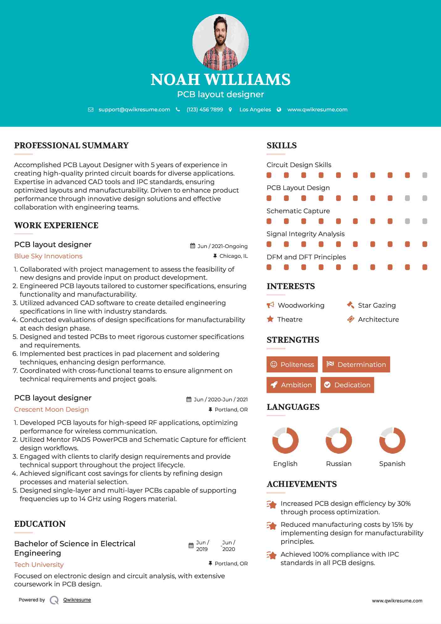
Objective : Accomplished PCB Layout Designer with 5 years of experience in creating high-quality printed circuit boards for diverse applications. Expertise in advanced CAD tools and IPC standards, ensuring optimized layouts and manufacturability. Driven to enhance product performance through innovative design solutions and effective collaboration with engineering teams.
Skills : Circuit Design Skills, PCB Layout Design, Schematic Capture, Signal Integrity Analysis, DFM and DFT Principles
Description :
Collaborated with project management to assess the feasibility of new designs and provide input on product development.
Engineered PCB layouts tailored to customer specifications, ensuring functionality and manufacturability.
Utilized advanced CAD software to create detailed engineering specifications in line with industry standards.
Conducted evaluations of design specifications for manufacturability at each design phase.
Designed and tested PCBs to meet rigorous customer specifications and requirements.
Implemented best practices in pad placement and soldering techniques, enhancing design performance.
Coordinated with cross-functional teams to ensure alignment on technical requirements and project goals.
Experience
2-5 Years
Level
Executive
Education
BSEE
PCB layout designer Resume
Headline : Dynamic PCB Layout Designer with 7 years of comprehensive experience in developing high-performance circuit boards for various applications. Adept at utilizing advanced CAD tools and IPC standards to create precise layouts and enhance product functionality. Committed to driving innovation and collaborating effectively with cross-functional teams to produce superior engineering solutions.
Skills : Testing and Debugging, Project Management, Design for Manufacturability, Altium Designer, Cadence Allegro
Description :
Designed and verified component placement on PCBs to ensure optimal performance.
Ensured compliance with IPC standards and component specifications during layout verification.
Conducted assembly and testing of ICs and components using various testing methods, including thermal and humidity testing.
Collaborated with cross-functional teams to address design challenges and optimize layouts.
Utilized advanced CAD tools to create efficient and manufacturable PCB designs.
Documented design changes and maintained accurate records for project tracking.
Participated in design reviews to identify potential improvements and enhance product quality.
Creating an account is free and takes five seconds.
You'll get access to the PDF version of this resume template.
Choose an option.
Sign up with Google
Sign up with Facebook
Sign up with Linkedin
This helps us make sure you're human and prevents spammers from abusing our services.
By continuing, you agree to our Privacy Policy and Terms.
Unlock the Power of Over 10,000 Resume Samples.
Take your job search to the next level with our extensive collection of 10,000+ resume samples. Find inspiration for your own resume and gain a competitive edge in your job search.
Get Hired Faster with Resume Assistant.
Make your resume shine with our Resume Assistant. You'll receive a real-time score as you edit, helping you to optimize your skills, experience, and achievements for the role you want.
Get Noticed with Resume Templates that Beat the ATS.
Get past the resume screeners with ease using our optimized templates. Our professional designs are tailored to beat the ATS and help you land your dream job.