A Digital Design Engineer designs new digital hardware products and also creates the circuitry which is needed for the product to operate and function. While specific duties vary based on the product that is being designed, the following are certain core tasks that are seen on a professional Digital Design Engineer Resume – testing and verifying circuitry such as mixed-signal circuitry; evaluating existing digital products and determining if changes or updates are to be made; creating surveys and working with customers; testing the products directly and determining its efficiency before it goes into the market, and documenting technical data.
Possessing the following skills are resourceful for career growth – strong analytical skills, the ability to stay up to date with the latest developments in the technology fields; critical thinking abilities and a thorough knowledge of the product that is being designed. A Master’s degree in electrical engineering or technology-related fields are mandatory.
Objective : Creative Digital Design Engineer with 2 years of hands-on experience in developing and optimizing digital systems. Proficient in VHDL and system-level design, with a track record of enhancing performance and reliability in integrated circuits. Passionate about leveraging innovative technologies to drive project success and deliver high-quality design solutions.
Skills : Fpga Development, System Verilog, Vhdl Programming, Fpga Design
Description :
Integrated modules for SERDES configuration and debug registers, enhancing system performance.
Authored comprehensive design specifications and user guides to streamline development.
Developed and executed detailed test plans for system validation.
Managed top-level integration and developed system test benches to ensure design reliability.
Created custom floor planning groups and regions, optimizing layout for timing performance.
Led post-silicon bring-up and lab debug, ensuring successful product launch.
Experience
0-2 Years
Level
Entry Level
Education
BSEE
Assistant Digital Design Engineer Resume
Objective : Innovative Digital Design Engineer with 2 years of experience in creating and refining digital systems. Skilled in VHDL and RTL design, focused on optimizing integrated circuit performance and reliability. Committed to applying advanced technologies to enhance design processes and deliver exceptional results.
Skills : Proficient In C Programming, Embedded Assembly Programming, Digital Circuit Design, Signal Processing, Embedded Systems
Description :
Led a team to enhance EDA design methodologies, improving design efficiency by 25%.
Developed and simulated architectural designs for a receiver modem, achieving a 15% increase in processing speed.
Engineered RTL interfaces for ADC and DAC systems, resulting in a 20% reduction in latency.
Executed synthesis and board-level testing of design modules, ensuring 100% compliance with specifications.
Develop and implement digital designs using VHDL and Verilog for FPGA and ASIC applications.
Collaborated on cross-functional teams to drive project success and innovation in digital design.
Experience
0-2 Years
Level
Junior
Education
BSEE
Digital Design Engineer Resume
Objective : Driven Digital Design Engineer with 2 years of experience in the development and optimization of digital systems. Adept in VHDL, RTL design, and system-level verification, contributing to enhanced performance in integrated circuits. Eager to implement cutting-edge technologies that elevate design quality and project outcomes.
Create and maintain design documentation, including specifications and test plans.
Executed RTL design and block-level verification for critical components, ensuring design integrity.
Participate in design reviews and provide constructive feedback to peers.
Implemented IO MUXes and clock divider blocks in Verilog, optimizing signal routing.
Built block-level test benches for key components from scratch, utilizing Verilog and C for comprehensive testing.
Developed directed and constrained random test cases, improving verification efficiency.
Conducted silicon validation to ensure design met performance specifications.
Experience
0-2 Years
Level
Entry Level
Education
BSEE
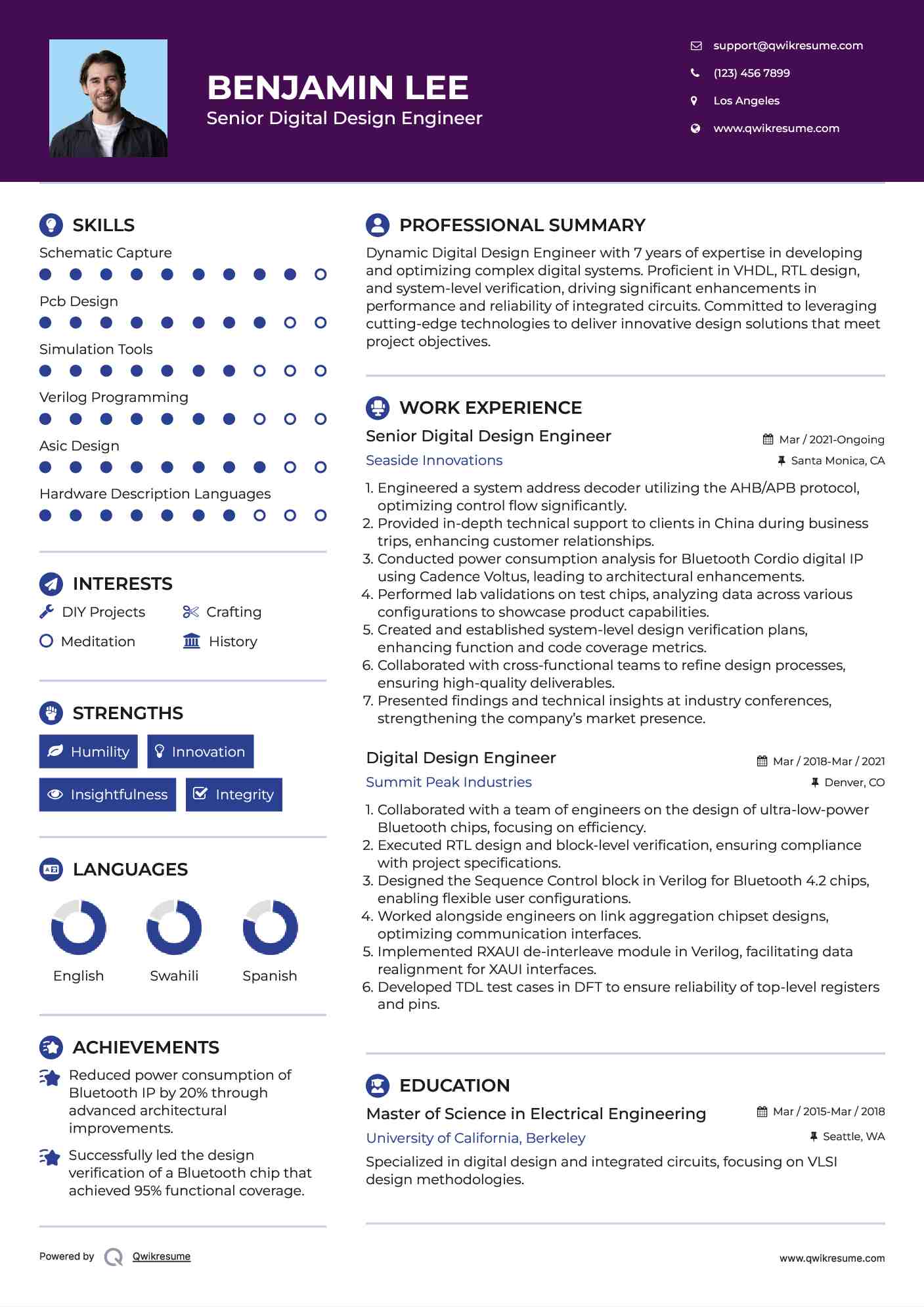
Senior Digital Design Engineer Resume
Headline : Dynamic Digital Design Engineer with 7 years of expertise in developing and optimizing complex digital systems. Proficient in VHDL, RTL design, and system-level verification, driving significant enhancements in performance and reliability of integrated circuits. Committed to leveraging cutting-edge technologies to deliver innovative design solutions that meet project objectives.
Engineered a system address decoder utilizing the AHB/APB protocol, optimizing control flow significantly.
Provided in-depth technical support to clients in China during business trips, enhancing customer relationships.
Conducted power consumption analysis for Bluetooth Cordio digital IP using Cadence Voltus, leading to architectural enhancements.
Performed lab validations on test chips, analyzing data across various configurations to showcase product capabilities.
Created and established system-level design verification plans, enhancing function and code coverage metrics.
Collaborated with cross-functional teams to refine design processes, ensuring high-quality deliverables.
Presented findings and technical insights at industry conferences, strengthening the company’s market presence.
Experience
5-7 Years
Level
Management
Education
M.S. EE
Digital Design Engineer Resume
Objective : Results-oriented Digital Design Engineer with 2 years of experience in the development and refinement of digital architectures. Expert in VHDL and RTL design, dedicated to enhancing integrated circuit functionality and efficiency. Excited to innovate and implement advanced technologies that streamline design processes and yield outstanding project outcomes.
Skills : Testbench Development, Design Verification, Fpga Prototyping, Power Analysis, Design For Testability, Analog Circuit Design
Description :
Engineered Flash Management Units (FMUs) for diverse automotive and industrial SoCs, optimizing on-chip Flash memory performance.
Implemented complex state machines and ARM microprocessors for enhanced functionality.
Focused on digital logic design, verification, and assembly-level firmware development.
Introduced innovative baseline hardware designs for rapid product derivatives.
Developed a pioneering program swap feature, facilitating quick application code updates with minimal downtime.
Revamped assembly code for a key product line, significantly reducing engineering time-to-market.
Led the resolution of intricate clock-domain crossing issues in multi-oscillator designs.
Experience
0-2 Years
Level
Entry Level
Education
BSEE
Associate Digital Design Engineer Resume
Objective : Results-driven Digital Design Engineer with over 5 years of experience in developing innovative digital circuits and systems. Proficient in VHDL/Verilog, FPGA design, and simulation tools. Strong background in signal processing and hardware-software integration. Committed to delivering high-quality designs on time while collaborating effectively with cross-functional teams to meet project goals.
Skills : Vhdl Design And Implementation, Vhdl Verification And Debugging, Problem Solving, Scripting For Automation In Design
Description :
Contributed to the development of a VHDL-based video processing system, enhancing data throughput.
Collaborated with cross-functional teams to ensure seamless integration of digital components.
Performed simulation and verification of designs, ensuring compliance with specifications.
Engaged in the design and implementation of digital filters to optimize signal quality.
Utilized version control systems to manage design changes and documentation.
Participated in design reviews and contributed to project planning and execution.
Assisted in the development of testing protocols to validate circuit performance.
Experience
0-2 Years
Level
Entry Level
Education
BSEE
Digital Design Engineer Resume
Objective : Accomplished Digital Design Engineer with 5 years of expertise in crafting and optimizing digital systems. Proficient in VHDL, Verilog, and FPGA design, I drive performance enhancements in integrated circuits. Passionate about integrating innovative technologies to deliver high-quality solutions that meet complex project requirements.
Skills : Timing Analysis, System On Chip, Mixed-signal Design, Design For Manufacturability, Layout Design, 3d Modeling
Description :
Utilize version control systems to manage design files and documentation.
Directed placement and routing of high-speed CCAs, developing instructions to optimize performance.
Engineered ARINC 429 and ARINC 717 interfaces, along with I2C and SPI communications.
Authored comprehensive DO-254 hardware plans and verification procedures.
Implemented PLL and VCO models in Verilog, enhancing test coverage and design robustness.
Provided technical expertise to the business development team, facilitating product outreach.
Participate in project planning and estimation of design timelines.
Experience
2-5 Years
Level
Junior
Education
BSEE
Senior Digital Design Engineer Resume
Headline : Accomplished Senior Digital Design Engineer with 7 years of extensive experience in crafting and optimizing advanced digital systems. Highly skilled in VHDL, RTL design, and FPGA implementation, I excel in enhancing performance and reliability of integrated circuits. Dedicated to utilizing innovative technologies to drive project success and deliver superior design solutions.
Designed and optimized high-performance digital systems using VHDL and Verilog.
Conducted comprehensive system-level verification to ensure reliability and functionality.
Collaborated with cross-functional teams to integrate innovative design solutions.
Developed and maintained detailed documentation for design processes and methodologies.
Utilized FPGA technologies to enhance design capabilities and performance metrics.
Implemented design improvements that resulted in significant cost savings and efficiency gains.
Mentored junior engineers in best practices for digital design and verification.
Experience
5-7 Years
Level
Senior
Education
MSEE
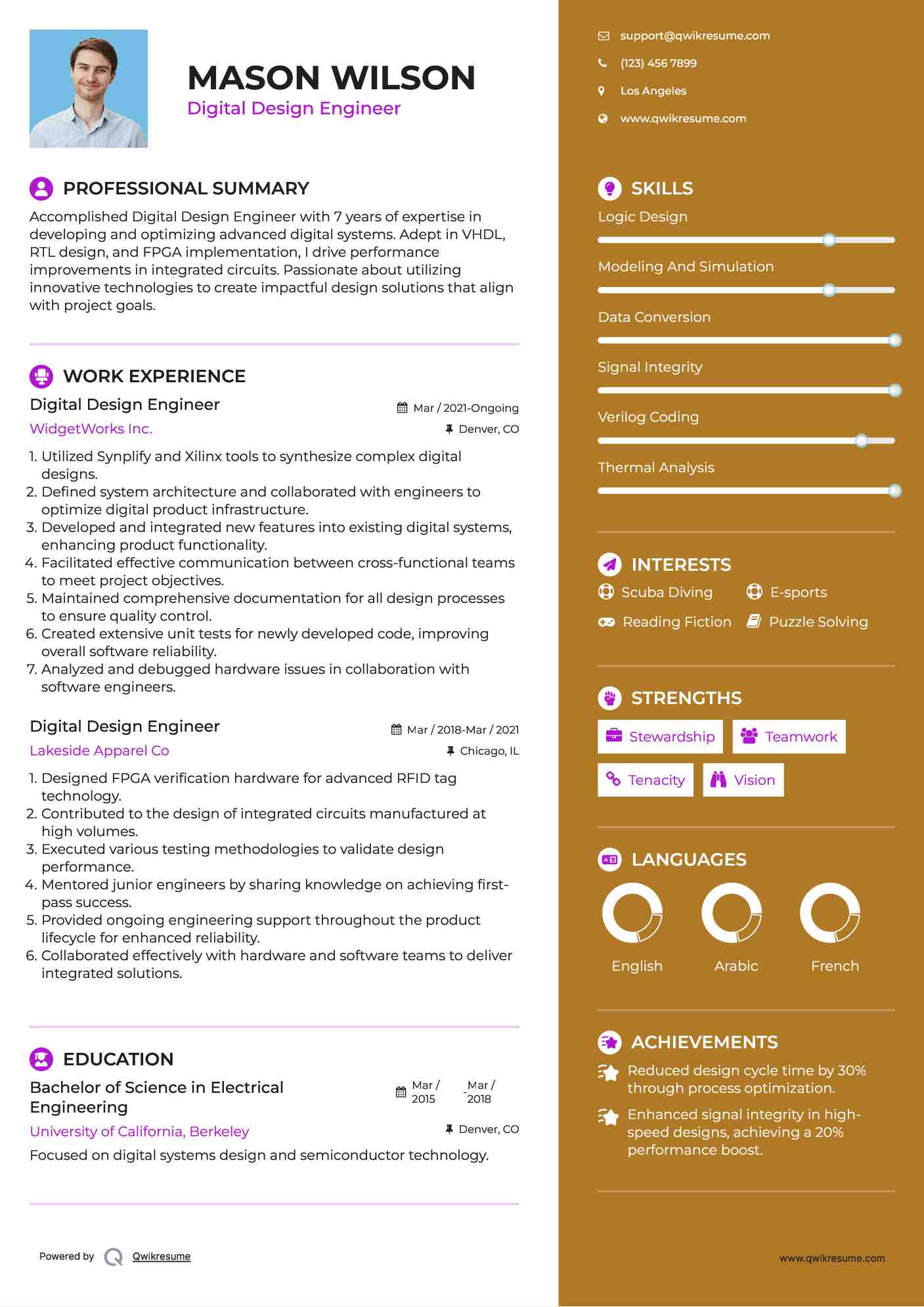
Digital Design Engineer Resume
Headline : Accomplished Digital Design Engineer with 7 years of expertise in developing and optimizing advanced digital systems. Adept in VHDL, RTL design, and FPGA implementation, I drive performance improvements in integrated circuits. Passionate about utilizing innovative technologies to create impactful design solutions that align with project goals.
Skills : Logic Design, Modeling And Simulation, Data Conversion, Signal Integrity, Verilog Coding, Thermal Analysis
Description :
Utilized Synplify and Xilinx tools to synthesize complex digital designs.
Defined system architecture and collaborated with engineers to optimize digital product infrastructure.
Developed and integrated new features into existing digital systems, enhancing product functionality.
Facilitated effective communication between cross-functional teams to meet project objectives.
Maintained comprehensive documentation for all design processes to ensure quality control.
Created extensive unit tests for newly developed code, improving overall software reliability.
Analyzed and debugged hardware issues in collaboration with software engineers.
Experience
5-7 Years
Level
Management
Education
BSEE
Digital Design Engineer Resume
Objective : Enthusiastic Digital Design Engineer with 2 years of experience in designing and optimizing digital systems. Skilled in VHDL and FPGA development, focused on enhancing the functionality and efficiency of integrated circuits. Eager to apply innovative methodologies and technologies to achieve superior design outcomes and contribute meaningfully to project success.
Skills : Firmware Development, Critical Thinking, Attention To Detail, Technical Communication, Team Leadership
Description :
Perform power analysis and optimization for digital circuits.
Engineered a new transceiver board improving compatibility with the Warrior logging system.
Redesigned receiver boards by integrating Altera FPGA, achieving a 25% improvement in measurement accuracy.
Created a high-performance lock-in amplifier utilizing analog devices DSP for array induction tools.
Designed multiple downhole logging tools, focusing on performance optimization and reliability.
Contributed to the design of the Warrior logging system, enhancing overall system functionality.
Engineered an advanced electromagnetic inspection tool to improve data quality and operational efficiency.
Creating an account is free and takes five seconds.
You'll get access to the PDF version of this resume template.
Choose an option.
Sign up with Google
Sign up with Facebook
Sign up with Linkedin
This helps us make sure you're human and prevents spammers from abusing our services.
By continuing, you agree to our Privacy Policy and Terms.
Unlock the Power of Over 10,000 Resume Samples.
Take your job search to the next level with our extensive collection of 10,000+ resume samples. Find inspiration for your own resume and gain a competitive edge in your job search.
Get Hired Faster with Resume Assistant.
Make your resume shine with our Resume Assistant. You'll receive a real-time score as you edit, helping you to optimize your skills, experience, and achievements for the role you want.
Get Noticed with Resume Templates that Beat the ATS.
Get past the resume screeners with ease using our optimized templates. Our professional designs are tailored to beat the ATS and help you land your dream job.
Build an ATS-friendly Digital Design Engineer Resume